PDu100 Micro Piezo Driver
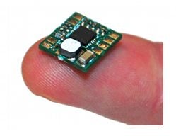
The PDu100 is an extremely small and lightweight driver for piezoelectric actuators. The PDu100 can drive two-wire piezoelectric actuators and benders up to +/-100 V. The PDu100 can also drive three-wire piezoelectric benders and stack actuators up to +100 V. Applications include battery powered robotics, piezoelectric motors, and ultra low-power positioning and manipulation systems.
The PDu100 is protected against short circuit, current overload, and excessive temperature. A shutdown pin is also provided that reduces the supply current to 1 mA when pulled low. The output voltage range and gain of the PDu100 is customizable to meet the requirements of OEM applications.
- Download Datasheet
Enquiry
Obtain instant quote
- Click Buy Now
- Select desired options
- Add to cart
- Proceed to checkout
- Enter details
- Download instant quote
Compatible Actuators
| Stack Actuators | up to 100V |
| Plates and Tubes | Up to +/-100V |
| Two Wire Benders | Up to +/-100V |
| Three Wire Benders | 0 to 100V with 100V bias |
Specifications
| Power Supply | 3 V to 5.5 V |
| Max Unipolar Output | +100 V |
| Max Bipolar Output | +/-100 V |
| RMS Output Current | 33 mA |
| Average DC Current | 15 mA |
| Power Bandwidth | 3.2 kHz |
| Peak Output Current | 100 mA |
| Signal Bandwidth | 60 kHz (unloaded) |
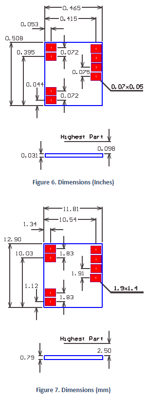
| Dimensions | 11.8 x 12.9 mm (0.46 x 0.51 in) |
| Weight | 560 mg (0.018 oz) |
| Gain | 27.5 V/V |
| Input Voltage | 0.5 Vs +/- 1.8V |
| Input Offset | +/-100 mV |
| Load Capacitance | Unlimited |
| Overload Protection | Thermal and current |
| Noise | 70mV RMS (10uF Load) |
| Environment | 0 to 70 C (-32 to 158 F) |
| Quiescent Current | 25 mA (1 mA in Shutdown) |
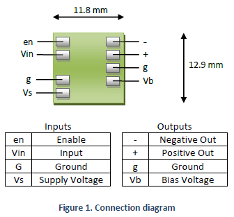
Connection Diagram
Operation
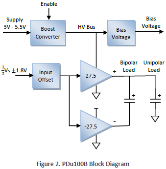
The system block diagram is illustrated in Figure 2. A boost converter generates a high-voltage rail to supply a pair of complementary amplifiers. A single output can be used to drive a unipolar load up to +100 V or both amplifiers can be used to produce +/-100 V.
The input is selectable between a unipolar signal biased at half the supply voltage or a bipolar signal. The amplifier gain is 27.5 so a 3.6 Vp-p input will produce a 100 Vp-p output. Both amplifier channels are biased at half the output range (50 V).
The overall system gain is determined by the output configuration. The possible combinations are listed below.
| Output Type | Gain | Input Range | Output Range |
| Unipolar | 27.5 | 0.5 Vs +/- 1.8V | 100 V |
| Bipolar | 55 | 0.5 Vs +/- 1.8V | +/-100 V |
System gain and voltage range
Both outputs are biased at approximately half the HV bus voltage, e.g. 50 V. The output voltage equations are listed below.
| Output Type | Output Equation |
| Unipolar | \( 27.5 \times \left(V_{in}-\frac{V_S}{2} \right) + 50 \) |
| Bipolar | \( 55 \times \left(V_{in}-\frac{V_S}{2} \right) \) |
System gain and voltage range
The gain and output voltage ranges can be customized by contacting info@piezodrive.com.
Example Applications
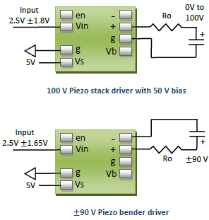
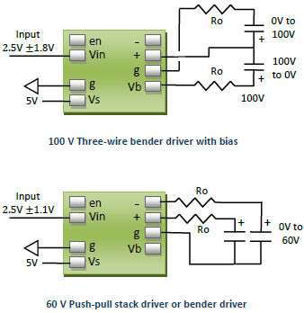
Some typical application circuits are shown below. The optional output resistance \( R_O \) is used to reduce noise as described in “Noise”. For general purpose applications, the recommended value for \( R_O \) is 270 Ohms.
Power Bandwidth
The power bandwidth is the maximum frequency periodic signal that can be reproduced without distortion. The power bandwidth calculator determines the maximum operating frequency and required power for a given load capacitance. The calculator includes the effects of current limit, slew-rate, and signal bandwidth.
The calculator does not include the time-constant of the peak current limit, and therefore may become inaccurate when the power bandwidth is below 50 Hz.
Noise
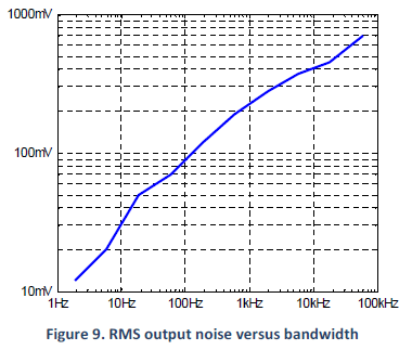
The output voltage of the PDu100 contains switching noise from the boost converter and random noise from the high-voltage amplifier. The amount of noise seen by the load capacitance is determined by the size of the output resistance and signal bandwidth. If there is no output resistance, a value of 100 Ohms can be used to calculate the bandwidth and predict noise.
To determine the output resistance required for a particular noise level, the required bandwidth should be selected from Figure 9 below. The correct resistance can then be calculated from
$$ R_O = \frac{1}{2 \pi f_{bw} C_L }$$
The noise measurements are performed with a static input voltage. When current is drawn from the output, the ripple will increase due to action from the boost converter.
Signal Bandwidth
The unloaded small signal bandwidth of the PDu100 is approximately 60 kHz. With a capacitive load, the signal bandwidth is determined by the output resistance, that is
$$ f_{bw} = \frac{1}{2 \pi R_0 C_L} .$$
Supply Current
The supply current \( I_S \) is related to the load current \( I_L \) through the following power balance equation
$$ I_S = I_L \frac{105}{ V_S \times 0.7} ,$$ where \( V_S \) is the supply voltage. With a capacitive load and sinusoidal voltage, the peak and average output current is
$$ I_{L(pk)} = \pi f C_L V_{L(p-p)} ,$$ $$ I_{L(av)} = 2 f C_L V_{L(p-p)} ,$$ where \( V_L \) is the peak to peak voltage across the load capacitance. The average supply current can be written $$ I_{S(av)} = 2 f C_L V_{L(p-p)} \frac{105}{V_S \times 0.7} .$$
Power Dissipation
With a capacitive load, power dissipation is the product of supply voltage and the average current, that is
$$ P_D = V_S \times I_{S(av)} $$ When operating at full power bandwidth, the worst-case power dissipation is approximately 2.5 W. The thermal impedance of the PDu100 from junction to ambient is 45 K/W . Therefore, the maximum temperature rise is approximately 90 degrees C above ambient.
When continuous power dissipation above 1 W is required, the PDu100 is designed to be mounted onto a thermal sink using a thermally conductive double-sided adhesive such as 3M 8940 or Bergquist BOND-PLY 100.
Enable / Shutdown
The Enable pin can be pulled low to disable the amplifier and reduce the quiescent current to 1 mA. It can be driven by a logic output or an open collector output. The recovery time after a shut-down is 2 ms.
Overload Protection
The PDu100 is protected against over-current and thermal overload. If the temperature exceeds 150 degrees C, the amplifier will be disabled until the temperature reduces.
